www.livescience.com
New 3D silicon chip stacks circuits on top of each other to boost computing power
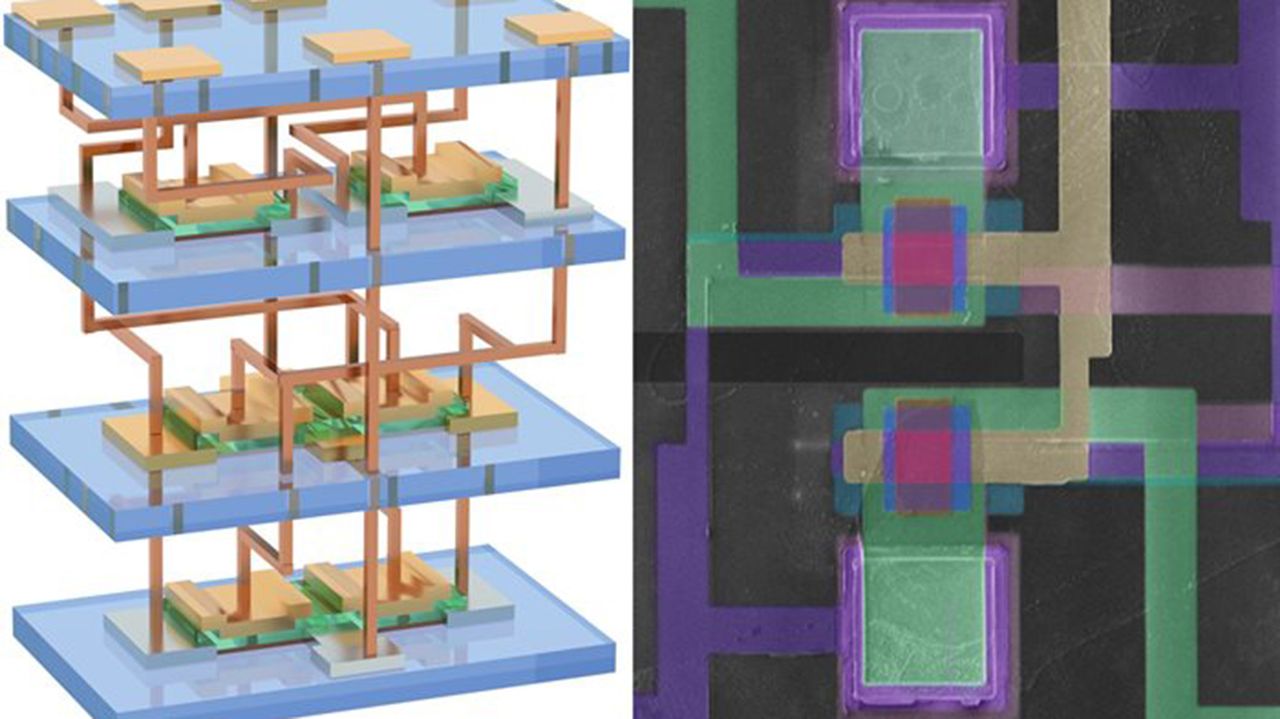
The massive hardware demands of artificial intelligence (AI) applications are stretching the physical and structural limitations of semiconductors. But researchers have engineered a three-dimensional silicon chip that they propose as the solution.In a new study published May 27 in the journal Nature, scientists found a way to cram more computing power into a chip by stacking silicon circuits in multiple layers in a way that doesn't impact performance. Stacking chips vertically, known as 3D integration, is more efficient than traditional 2D chips, where silicon circuits are spread across a single surface. This is because stacking shortens the distance that data has to travel and reduces the power required for data transmission.The researchers' 3D chip uses ultrathin silicon membranes and low-temperature manufacturing techniques to overcome the challenges of current chip architectures. "Our method is not only easier to implement with lower cost, but it has several advantages over previous approaches to stack silicon wafers," Qing Cao, first author of the study and a materials science and engineering professor at the University of Illinois Urbana-Champaign, said in a statement.Extending Moore's lawSince the 1960s, ensuring that electronics can handle more demanding applications has meant making transistors smaller so more can be packed onto a single chip. But, as Cao pointed out, doubling the number of transistors every couple of years — a principle known as Moore's law — is becoming less feasible."If you look at the actual size of transistors, they're not getting smaller, especially in terms of their contacted gate pitch," Cao said in the statement — defined as the combined width of one transistor gate and the space needed to separate it from the next. "This is because we're becoming limited by the intrinsic material properties of silicon and the fundamental rules of quantum mechanics. If we're going to keep up the trend of increasing processing power of our microprocessors, we have to start thinking beyond just squeezing more devices on a single surface."The researchers think vertical integration across multiple layers is the best way to guarantee that engineers can continue to adhere to Moore's law, because this approach creates room for more transistors on a chip. "Today it takes six microelectronic devices called transistors on a single plane to store one bit of information," Cao explained, suggesting that just like in a densely populated city, the only way to solve overcrowding is to build upward. "You get the same functionality, but the spatial footprint is reduced while making communication between layers faster and more efficient."Scientist Gordon Moore seen with a graph representing Moore's Law. (Image credit: Intel)Getting around the heat problem Stacking is nothing new, of course, but vertical integration — building layers directly on top of one another — can create thermally dense packages. In the study, the researchers noted that the fabrication of high-quality silicon chips demands temperatures up to 1,832 degrees Fahrenheit (1,000 degrees Celsius). However, once the first chip layer has been completed, the metal wiring introduced to connect further layers can be destroyed by such high temperatures. As a result, the "thermal budget" — the maximum amount of heat that can be endured before degradation starts to occur — for any additional layers is 752 F (400 C), said Cao. This can result in performance and reliability issues.When creating 3D stacked silicon chips, manufacturers have sought to avoid this problem by using alternatives to single-crystalline silicon for the upper layers, according to the researchers. These materials include amorphous and nanocrystalline metal oxides, carbon nanotubes and polycrystalline silicon, but they can lead to performance and reliability issues, the scientists said in the study. To overcome this challenge, Cao and his team adopted an approach called "monolithic integration" — a process in which all chip components are fabricated on a single piece of substrate, as opposed to making them separately and then bonding them together later. To build each chip, the researchers created ultrathin silicon nanomembranes that they then transferred, using a roll laminator, onto a substrate containing the bottom layer. Related storiesScientists say they've eliminated a major AI bottleneck — now they can process calculations 'at the speed of light'Scientists trained an AI model using an IBM quantum computer — and it answered questions correctly that the base model couldn'tWhat's the biggest bottleneck to building better AI? It's no longer the lack of computing resources — it's generating enough energy to feed itThe maximum temperature required to generate a strong bond using this method was just 392 F (200 C) — five times less than the heat normally required. The membranes they transferred were also just 10 nanometers thick or less — about the size of a protein — compared with the approximately 500-to-700-micrometer (500,000 to 700,000 nanometers) thickness of a typical wafer. Because they are thin, these membranes are mechanically flexible to conform to the underlying surface, Cao added. The result of this process was a 3D chip with three layers, each containing 625 transistors. This pales in comparison to the billions of transistors that can be crammed onto chips already on the market, but the researchers believe their technology boasts power efficiency benefits. The electrical current that can flow through the chip has proved to be at least three to four times greater than that of monolithic chips made from alternative materials.The big question is whether their 3D silicon chip can make the leap from the laboratory to commercial applications. While the research demonstrates the potential of a chip comprising three stacked layers, the scientists suggested that plenty more layers can be added in future iterations.Can you match these ancient devices to their pictures? Find out with our computing quiz!








 New Posts (Home)
 ChatBox
 Popular Posts
  Game Zone
 Top PodCasts